dimanche 17 novembre 2024

EMU 1 : First attempt to write a program for the EMU1 motherboard

As I indicated in my previous post, I now need to know if the DRAM on the EMU1 motherboard is fully functional or not.

As a reminder, when I had this EMU1, a few years ago, I was able to load a sound disk without the slightest problem. Then the machine smoked. Nothing serious, a few tantalum capacitors shorted. I replaced these capacitors and reassembled the machine without ever being able to restart it. Since then, it has never managed to read a diskette. So I had tested all the DRAM components with a small tester which had not indicated any faulty components.

Due to the multiplexing mechanism of the DRAM address bus, using 'criminal' timings performed with resistors/capacitors, I am therefore trying to get an idea of how this system currently works.

To do this, I will write a very simple program whose goal will be to represent on a series of LEDs connected to an output port of the EMU1 motherboard, the evolution of a simple 8-bit counter.


This program, of rare complexity, simply increments an Index whose value will be sent to the IO address space 0xC0 (__sfr __at 0xC0), in a loop slowed down by a timer consisting of two nested empty loops. There is no prior initialization of the Z80 registers. I do not use IRQs or the memory stack.

This simple program requires 5 bytes of RAM memory. If it works, it will already indicate that the DRAM components are being accessed 'relatively' correctly. If this program works, I will modify it to test the entire 128KB of RAM.

I compile this program using SDCC and the command:

sdcc -mz80 --no-std-crt0 --vc --code-loc 0x0000 --data-loc 0x400 TestRam.c

No special comments. The code starts at address 0x0000 and continues and uses only a few bytes of program area. The data in RAM will be positioned from address 0x0400, just at the beginning of the RAM space, just behind the first KB of code.

And now??? Well, we need to encode the content of the ROM code obtained after compilation and conversion into a binary file to make it compatible with the wiring system made by EMU (thanks EMU)!

Even for a few bytes of ROM, I preferred to write a small program under Windows to automate the task. Because it is necessary to encode not only the data but also the addresses. So as I plan to expand this small test program, I might as well make this encoding process as automatic as possible, even if it means 'taking' a little time to write the Windows application.

I hate using Microsoft's Visual C++. A gas factory, a big piece of crap (for me, because there are thousands of programmers who love Visual C++), GB of data to load and never knowing where we're going! So I tried it with QT. Its mode of operation is much more logical/simpler/efficient for me. Starting with no knowledge of QT, I 'only' needed a short day (I program embedded and am very bad with OS applications) of discovery to be able to write a minimal application that suits me.


So I know that the original EMU executable is 60 bytes. It's 'big' for such a small program, but I coded it in 'C' and not directly in assembler.

And for comparison, here is what the contents of the original binary file look like :


And now the binary encoded in the EMU 'way':


Well, if I understood correctly how the EMU1 motherboard works, if I also understood correctly the ROM coding system and if the DRAM multiplexing system is correct, it is not impossible that I can see something on the LED connector. Maybe not the progress of the counter if my temporisation is not sufficient, but still something...

Now I just have to program a 2732, put it on the motherboard, connect an LED and see if anything happens.

The result of my investigations in a future post...

mercredi 13 novembre 2024

EMU 1 : blocked for now

In my previous post, I stuck to the fact that the EMU1 motherboard was now able to start the floppy drive as well as return the read head to track zero. However, I still had no real boot from the motherboard.

From what I was able to read from the EMU doc, in principle the bios reads the first track, which obviously contains a more sophisticated bootloader than the one contained in the EPROM, therefore records this first track somewhere in RAM, then executes this piece of code whose objective is to read the entire contents of the floppy disk.

However, even with a floppy disk supposed to contain the necessary files, the contents are not read. Which therefore indicates that the first track is not read correctly, or that its loading and execution from RAM is not going well.

Since I think the SIO and PIO system now works for floppy disk drive and reading, I decided to take a closer look at the signals from the dynamic RAM. And as a result, I was able to see that the pin 3 of the RAMs had a level that never varied.


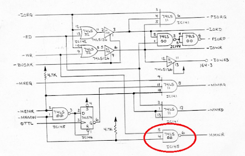
All these signals are driven by the signal noted MMWR. This signal comes from the logic for managing the types of memories accessed.


And indeed whatever the levels present on inputs 4 & 5 of the NAND gate, output 6 does not move. So I removed this IC145 circuit from the EMU board and positioned it on the EPROM programmer, which also acts as a logic integrated circuit tester, and the test result is that everything is good.


Hmm, skeptical! I therefore replaced this circuit with a new 74HCT00 that I own and as was predictable, I found activity on pin 6. The MMWR signal therefore became valid again.


From my first tests years ago on this motherboard, I started by testing as many integrated circuits as possible this way, so I put this 74LS00 back in place since it was supposed to be in good condition. As a result, now, I no longer have any certainty about the other components tested in this way, which still represents almost 90% of the components.

And now? Well, I'm supposed to have a motherboard with a working floppy drive system, as well as a working DRAM. And yet, the OS still does not load from the floppy disk, knowing that I respected the minimum configurations of the mother board for it to work.

However, this EMU motherboard contains an absolutely horrible and totally prohibited solution when it comes to logic circuits: the creation of delays using resistors and capacitors. Here is the 'crime' scene:


The principle is easily understood. First, part of the address bits are sent to the RAx pins of the DRAMs. Then, some time later, the other address bits are presented to the RAx pins of the DRAMs. Then, some time later, again, the validation of this second part of the address is validated by the CAS signal. The selection of the address bits is done with the 100Ohm resistor and the 220pF capacitor, the activation of the CAS signal is done with the 200Ohm resistor and the 680pF capacitor.

I was actually able to check with the oscilloscope that the timing was respected. But, due to the uncertainty of the real level of taking into account the levels by the different circuits, and especially the possible drift in capacitor capacity over time, I am, in the current state of things, totally incapable of tell if the current timing of the signals fits within the specifications of the DRAM packages. If this is not the case, obviously the bytes read from the floppy disk cannot be stored/read correctly in memory.

And so here I am again blocked by too many uncertainties. Obviously, if I had been able to get my hands on the dynamic memory test EPROM, it would have allowed me to quickly get an idea. On the contrary, if I want to move forward efficiently, I need to create a small program whose purpose will be to write a byte to the extent of the memory, and to check its presence when reading. This should allow me to first check if anything is wrong.

And to do it well, I would even have to configure the serial interface of the SIO dedicated to the connection with a computer to allow the display of a few messages including, if possible, the location of the DRAM circuit affected by a writing/reading problem. Creating this type of program does not pose any difficulty, however, it is still necessary to code the generated binary in both bit order and address order, to match the 'esoteric' wiring of the EPROM on the processor.

At the same time, this type of exercise could allow me to also program some operating tests for the PIO, the SIO, the CTC and possibly the DMA controllers...

vendredi 8 novembre 2024

EMU1 : some progress...

In the previous post on this subject, I had stopped at the fact that I had discovered that the wiring of the EPROM to the processor did not respect the conventions. I therefore confirm this fact, and am even able to say that all EMU1 motherboards have this characteristic which can be defined as a relatively simple coding of the EPROM whose purpose is, I think, to make the disassembly of the program difficult.

To come to this conclusion, I read the original EPROM from my EMU1 motherboard. To do this, I placed the EPROM on a circuit socket from which I cut off the +12V and -5V power supply pins. Because the MiniPro is not able to provide these power supplies on these pins. So I was able to connect these two EPROM pins directly to an external laboratory power supply.

MiniPro


Socket adaptor

In fact, in order to be able to test the operation of this motherboard, I had originally removed the +12V and -5V power supply from this EPROM. The goal was to be able to eventually test the operation of the board with another version of the boot program. This also allowed me to check the behavior with the logic analyzer and draw my conclusions as to how this EPROM is connected to the processor.

Note that to read the EPROM on the MiniPro, I selected a 2716 type EPROM, the smallest available on the software, knowing that I would therefore have twice the same KB read since the original EPROM is a 2708 and the additional address bit of a 2716 is not connected to the 2708.

So, now that I am sure that the motherboard of this EMU1 works, since it is able to execute my 'NOP' loop, I need to continue on the right basis, that is to say, program a 2732 that I have with the original EPROM program and insert this 2732 in place of the original 2708.

On the other hand, EMU strongly advises to always use the original EPROM to perform tests. So...


I don't know why this exists, but I strongly suspect it has to do with some hardware feature. Since the boot program just reads the first track of the floppy anyway and then runs this firmware to load the entire floppy, I suspect it has to do with just some basic motherboard functions. I don't know more than that at this point. Potentially setting a timer?

In fact, I compared the contents of the EPROM of my EMU1 board with other contents of different versions found on the Internet, I noted different codes at the addresses:
0x208
0x228
0x237
At least, the code in 0x237 is different on all the contents. The 4-voices version also has a difference in 0x208, and the Wildcard version, has the 3 differences.

Be careful, these codes at these addresses do not mean anything. They correspond to a specific code at a specific location, but after reorganization of the code according to the wiring of the EPROM to the processor.

The versions tested were the following:

600X.PROM(c)82_820816_#008D.BIN (The one on my board)
820816-00B8.bin
820816-0081.bin
820816-0165.bin
820816-0181.bin
E14Voice2708.BIN
Emu_wildcard.bin

At this point, and after inserting an EPROM containing the original boot program of my EMU board, nothing happens at the floppy drive. On the EMU1 board, the voice DMA controllers are not inserted. Only the principal DMA controller is inserted on its socket. In this configuration, I know that the boot program starts and runs. Despite the fact that this situation is not optimal for the minimal operation of the motherboard, something should still happen at the floppy drive, namely at least the rotation of the disk. However, nothing happens.

And this is when I change the first component that I think is defective on my board, namely the SIO. In fact, it is this SIO that generates the floppy drive selection signal, which has the effect of starting the floppy disk rotation motor. 


After this intervention, indeed, the rotation motor starts correctly. This is a good start, but nothing else happens. However, before anything else, in any procedure for reading a floppy disk, the controller must ensure that the reading head has returned to its initial position. Three signals are then important, the movement direction signal, the control signal for the stepper motor for positioning the reading head, and the track 0 position return signal. And these signals are managed not by the board's SIO, but by the PIO.


So I also replace this PIO.

After replacing these two components, indeed, by powering the motherboard back on, randomly, the floppy drive not only starts, but its head moves slightly to test the positioning of track 0. So I am also on the right track!

Of course, at this point I can't avoid to ask myself a few questions. How come the two interface components with the floppy drive are defective? On my workbench, the system is in the same configuration as in the EMU1 box. Is there a power supply problem in the EMU1? Because on my workbench, everything is powered by a laboratory power supply. Before reassembling this EMU1, I had obviously checked the proper functioning of the power supply that I had recapped. Strange all that!!!

Well, now I have a system that seems to boot properly from time to time. That is, it boots the floppy drive and sets the read head to track 0. But nothing more. The randomness doesn't surprise me either. The current configuration of the DMA components is not good at all. Besides, I'm now dealing with these DMAs.


It may not be very obvious at first glance, but the DMA system takes care of all data transfers with the floppy disk drive, in addition to managing the sound by sending the samples to the digital/analog conversion boards.

And, a quick reading of the schematic indicates that it is the first channel of the first DMA controller for reading samples that is used. Quite simply by assigning its signals, not to the conversion board, but to the floppy drive when accessing this drive. In order to make the board undisturbed by the absence of the conversion boards, I therefore position certain signals to ground, as indicated on the schematic provided by EMU. In fact, I only keep the first DMA controller and I remove any random character of a DMA trigger by the conversion boards.


In fact, I only leave the DMA controller #1 (I'm not talking about the head one which must be in place anyway). This is materialized by grounding some signals on the EMU1 motherboard.


Well, it's not meant to stay like this in the long term ;-)

And now I can power up this great EMU1 board again. Good 'surprise', the boot sequence now runs correctly and in the same way after each RESET of the board. The disk rotation motor starts, the reading head is positioned at track zero, even when I previously moved it by hand.

But for now, the situation seems frozen in this state. According to the EMU documentation, track 0 should be read then saved in RAM then executed to completely load the floppy disk. I performed my tests with a floppy disk containing the system but nothing works. I now need to check with the oscilloscope that the data from the floppy disk arrives correctly at the SIO of the EMU1 motherboard.

So I also have to deal with the interrupt management chain because it may 'block' at that level. I imagine that the SIO generates some of them, in any case it is wired for that and even has the maximum priority. A priori the interrupt chain stops at the PIO, the DMA controllers do not manage interrupts in this system.

This is the next step. It's laborious, but it's progressing!

jeudi 31 octobre 2024

EMU, oh no!!! Why???

After investigations of all kinds, still impossible to find an entry point on the non-functioning of this EMU 1, but...

Until now, I have taken the subject in a 'scientific' way. That is to say, by systematically controlling the operation of the processor. Despite the number of hours which is now starting to rise, not only do I not understand what is happening, but the result of what I observed really perplexes me!

Alas, must I say that I have now to move on to another study methodology: place to the artistic side of my brain! 

And, as a result, I am forced to let my mind wander at its own pace, without really commanding it. I have no idea of ​​the direction my ellucubrations will take. On the other hand, I think it will take some time...

So, and I can't really explain the entire thought pattern that I followed to arrive at the current result, but the fact remains that I finally arrived at the first result.

What is it about? I can get 'nothing' to run on the Z80 processor. Isn't it beautiful?

After many negative results, I tried to execute a NOP (No OPeration) loop on the entire ROM area of ​​the system, with looping at address 0x0000.

Well this simple 'trick' didn't work. On the other hand, I was able to note with the logic analyzer the repetition of a value at regular intervals. Not the right value, and not the right tempo!!!

SO? Well I carried out some connection tests on the processor board, and I noticed that it does not correspond at all to the diagram that I was able to obtain for this board. So obviously, I'm not sure that the schematic I have corresponds to version 4 of my motherboard. But, even so, some connections are, how can I put it, baroque!

And at this stage, to ask the developers of this EMU 1 (if any is still alive): but why? To avoid copying the machine too simply? But no... It's of no use, except to stall 'some' time for anyone trying to troubleshoot an EMU 1 :-(

So, perhaps, in the context of the times (1982), it was probably not easy to find a personal computer capable of assembling Z80 code, encoding the result so that it could be properly executed by the Z80. But hey, that’s debatable. On the other hand, this makes it completely impossible to disassemble the PROM. But on the one hand, this doesn't fool anyone with Z80 experience, and then you 'just' have to find an EMU 1 and study the motherboard to find the 'trick'. That's what I did. And frankly, finding only one OUT statement in all the code is just not credible, and that set me off ;-)

In short, once I understood the 'false' problem, I coded the PROM correctly and inserted it into its socket on the EMU 1 processor board. And you know what? With the logic analyzer, I found the code 0xC3 (JUMP) at the regular interval of 1024 bytes. Which proves to me that, for the first time, this board is able to execute an empty loop correctly.


No but, frankly, EMU! :-(

Now I can turn to the four DMA circuits that equip this motherboard. In fact there are five, but only the four 'slaves' cause problems on the data bus when they are on their socket. I will focus on their operation because that is what my brain is now telling me to go and check. So....


jeudi 17 octobre 2024

During this time...

I'm currently waiting for some printed circuit boards, and since I'm on the Drumulator topic, I decided to try to troubleshoot another machine from EMU: the Emulator 1.

This machine was offered to me by someone who wanted to part with it. It had obviously suffered some damage to the frame, following a fall I imagine, because it is really very heavy.

I turned it on once. It started, it smoked, then nothing since then. In fact it was tantalum capacitors that smoked. Nothing serious a priori.

In the past, I took it all apart and changed the front panel capacitors. I also redid the power supply. Then, I put everything back together, scrupulously, and then nothing. This EMU never wanted to restart. The keyboard has been sitting in a corner of my workshop for years. So, having studied the Z80 processor quite a bit during my work on FPGA, I thought it might be interesting to start troubleshooting it. After all, I have managed to troubleshoot several Drumulatore and SP12!


The interior of this EMU1 is in very good condition. Given the 'historical' nature of this machine, I find it increasingly difficult to look at it half dying in its corner!

So I removed the motherboard from the machine once again.


Will I finally be able to boot this motherboard from its floppy drive? The question remains!


It starts badly, the disk rotation motor gives a very slight knock and then stops. I have already spent some time checking the functioning of the motherboard by testing the behavior of the components. And, while I have already done this work years ago, I can't find anything dysfunctional. I don't have a diagnostic ROM for this machine, so for now, it's just a matter of testing the components. I haven't noticed anything glaring. Now I have to try to discover a functional malfunction. This is not going to be easy and may take a lot of time. But hey, I figure that by working on the subject a little regularly, I should get there! This machine only has standard components so....

vendredi 11 octobre 2024

MIDI SWITCH.

I have been thinking about developing 'simple' hardware for MIDI network management for years. In fact, I have been thinking about this for decades now!

I remember starting to develop a prototype based on a 68000 processor and two large communication circuits equipped with four serial ports each. That was in 1994, exactly thirty years ago!

I never got anywhere because, I don't know, subconsciously I found that there was something wrong.

In fact, I always started from the same paradigm, namely, a centralized element for the management of all MIDI communications.

And precisely, in the last few days, while I am currently rethinking all the wiring of my hardware in MIDI, a kind of evidence presented itself to me. Not an evidence on what to do, but only an evidence on what not to do. Exactly what I have always done, always starting from the same concept.

As you can imagine, the result I arrived at does not correspond at all to what I was doing until now.

So I present to you just a small piece of the printed circuit of what will be my MIDI network flexibility device :


Simple, right?

Of course, the hardware aspect is not everything. It will also be necessary to develop the right software, because the information management will be a little more complicated than with the standard MIDI network. But nothing too esoteric nevertheless.

I am hopeful that with this solution, I will finally be able to use all my MIDI machines without having to rack my brains every time I want to do something, nor having to unplug and replug inaccessible cables, equipped with this 'crappy' DIN plug!

lundi 7 octobre 2024

Drumulator and Efinix FPGA.

The fact is that I have made good progress on the transcription of the Drumulator into an FPGA.

But what craftsmanship job is the management of vectorized interruptions on the Z80! It 'smells' like the thing put in place last, with the resources still available for the circuit, and added on top of the logic of the processor itself! 

Well, that's the effect it has on me. So, it's a bit complicated to create a circuit that responds to this mechanism, especially the CTC circuit, very important in the Drumulator. I still got there.

But another problem arises. I wanted to recover the values ​​of the display digits in registers in order to be able to exploit them as I wanted, but using the small resources of the FPGA development board, I absolutely cannot get an idea of ​​how the multiplexing of the display is set up.

Obviously, everyone knows the principle of multiplexing, and basically, it works in the standard way on the Drumulator, but I retrieve multiple information in the registers. So, and as I have already set up the display of the Dumulator on an FPGA board equipped with 7-segment displays, I decided to create a small display/keyboard card functioning in the same way as the hardware implemented on the Drumulator. And in any case this card will allow me to work more easily with the Efinix FPGA board because it only has 8 user LEDs in total: it's really too few and it's a real criticism that the 'we can do with this board.

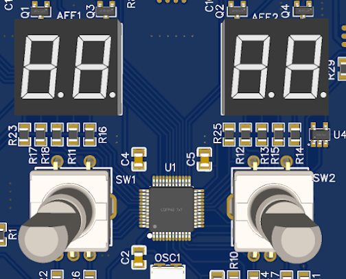
Here is what I sent to be done:


Although the Drumulator display only has 4 digits, I implemented 8, which will allow me to also display other debugging information if necessary.

So I'm putting this topic in standby until I receive the printed circuit  board and can mount and test this display/keyboard card.