In my previous post, I stuck to the fact that the EMU1 motherboard was now able to start the floppy drive as well as return the read head to track zero. However, I still had no real boot from the motherboard.
From what I was able to read from the EMU doc, in principle the bios reads the first track, which obviously contains a more sophisticated bootloader than the one contained in the EPROM, therefore records this first track somewhere in RAM, then executes this piece of code whose objective is to read the entire contents of the floppy disk.
However, even with a floppy disk supposed to contain the necessary files, the contents are not read. Which therefore indicates that the first track is not read correctly, or that its loading and execution from RAM is not going well.
Since I think the SIO and PIO system now works for floppy disk drive and reading, I decided to take a closer look at the signals from the dynamic RAM. And as a result, I was able to see that the pin 3 of the RAMs had a level that never varied.
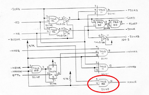
All these signals are driven by the signal noted MMWR. This signal comes from the logic for managing the types of memories accessed.
And indeed whatever the levels present on inputs 4 & 5 of the NAND gate, output 6 does not move. So I removed this IC145 circuit from the EMU board and positioned it on the EPROM programmer, which also acts as a logic integrated circuit tester, and the test result is that everything is good.
Hmm, skeptical! I therefore replaced this circuit with a new 74HCT00 that I own and as was predictable, I found activity on pin 6. The MMWR signal therefore became valid again.
From my first tests years ago on this motherboard, I started by testing as many integrated circuits as possible this way, so I put this 74LS00 back in place since it was supposed to be in good condition. As a result, now, I no longer have any certainty about the other components tested in this way, which still represents almost 90% of the components.
And now? Well, I'm supposed to have a motherboard with a working floppy drive system, as well as a working DRAM. And yet, the OS still does not load from the floppy disk, knowing that I respected the minimum configurations of the mother board for it to work.
However, this EMU motherboard contains an absolutely horrible and totally prohibited solution when it comes to logic circuits: the creation of delays using resistors and capacitors. Here is the 'crime' scene:
The principle is easily understood. First, part of the address bits are sent to the RAx pins of the DRAMs. Then, some time later, the other address bits are presented to the RAx pins of the DRAMs. Then, some time later, again, the validation of this second part of the address is validated by the CAS signal. The selection of the address bits is done with the 100Ohm resistor and the 220pF capacitor, the activation of the CAS signal is done with the 200Ohm resistor and the 680pF capacitor.
I was actually able to check with the oscilloscope that the timing was respected. But, due to the uncertainty of the real level of taking into account the levels by the different circuits, and especially the possible drift in capacitor capacity over time, I am, in the current state of things, totally incapable of tell if the current timing of the signals fits within the specifications of the DRAM packages. If this is not the case, obviously the bytes read from the floppy disk cannot be stored/read correctly in memory.
And so here I am again blocked by too many uncertainties. Obviously, if I had been able to get my hands on the dynamic memory test EPROM, it would have allowed me to quickly get an idea. On the contrary, if I want to move forward efficiently, I need to create a small program whose purpose will be to write a byte to the extent of the memory, and to check its presence when reading. This should allow me to first check if anything is wrong.
And to do it well, I would even have to configure the serial interface of the SIO dedicated to the connection with a computer to allow the display of a few messages including, if possible, the location of the DRAM circuit affected by a writing/reading problem. Creating this type of program does not pose any difficulty, however, it is still necessary to code the generated binary in both bit order and address order, to match the 'esoteric' wiring of the EPROM on the processor.
At the same time, this type of exercise could allow me to also program some operating tests for the PIO, the SIO, the CTC and possibly the DMA controllers...


Très intéressant ;) à bientôt Philippe
RépondreSupprimer